With burgeoning demand for high-performance artificial intelligence chips, back-end process technology, which assembles various semiconductors and tests the functionality of such chips, has become more important than ever.
So, it’s no wonder leading contract chipmakers such as Taiwan Semiconductor Manufacturing Company (TSMC), Samsung Electronics Co. and SK Hynix Inc. are going all out to advance or secure advanced technology for chip packaging – one of the final steps in semiconductor manufacturing.
Hana Micron Inc., a South Korea-based back-end process specialist, is one of those firms that take on globally renowned rivals with their hidden technologies.
Hana Micron is Korea’s top back-end process firm, also known as an outsourced semiconductor assembly and test (OSAT) company.
Hana Micron is South Korea's leading chip packaging company (Captured from Hana's website) The company is currently developing a 2.5D packaging technology that horizontally assembles different types of AI chips such as high bandwidth memory (HBM).
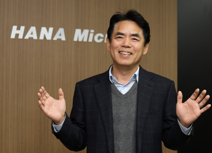
“We’re staking our future on advanced 2.5D packing tech for HBM and other AI chips,” said Chief Executive Lee Dong-cheol during a recent interview with The Korea Economic Daily.
In his office at Hana’s R&D center located in Pangyo, Korea’s Silicon Valley, Lee said the chip packaging technology currently under development is crucial for producing AI chips such as Nvidia Corp.’s H100 AI accelerator.
“TSMC has already secured the 2.5D packaging tech for H100. Samsung and SK Hynix and a few back-end companies are close to it. We, Hana Micron, have also produced prototypes,” he said. He added, however, that it may take some time for Hana to reach the full-scale commercialization stage.
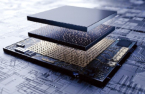
Samsung's 3D chip stacking technology, X-Cube PACKAGING: NEXT BATTLEFIELD
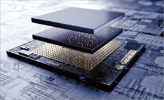
Packaging places chips in a protective case to prevent corrosion and provides an interface to combine and connect already-made chips.
Leading foundry players such as TSMC, Samsung and Intel Corp. are fiercely competing for advanced packaging, which allows multiple devices to be merged and packaged as a single electronic device.
Packaging technology can enhance semiconductor performance without having to shrink the nanometer through ultra-fine processing, which is technologically challenging and requires more time.
Demand for such technology is rapidly increasing in line with growth in generative AI such as ChatGPT, which requires semiconductors that can process large data quickly.
According to consulting firm Yole Intelligence, the global chip packaging market, including 2.5D and more advanced 3D packaging, is forecast to grow from $44.3 billion in 2022 to $78.6 billion by 2028.
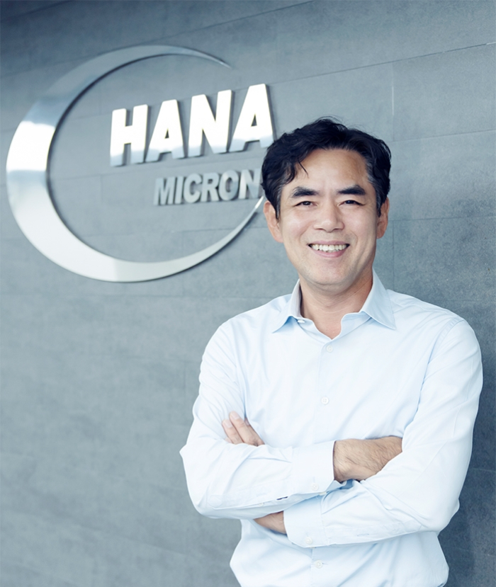
Hana Micron CEO Lee Dong-cheol HANA MICRON’S VIETNAM BUSINESS
Established in August 2001, Hana Micron operates production facilities in Korea, Vietnam and Brazil and runs overseas sales operations in the US, Vietnam and Brazil.
It is offering a packaging turnkey service, handling the entire process from chip packaging to module tests. It counts Samsung, SK Hynix and the Netherlands-based NXP Semiconductors among its clients.
Listed on Korea’s tech-heavy Kosdaq market, the company is particularly expanding its business in Vietnam.
Since it entered the Southeast Asian market by launching a corporation in Bac Ninh Province in 2016, Hana Micron has invested heavily, bringing its monthly production of packaged chips to 50 million units now.
The company plans to raise the monthly output volume to 200 million by 2025 with a cumulative investment of up to 700 billion won ($525 million) since 2016.
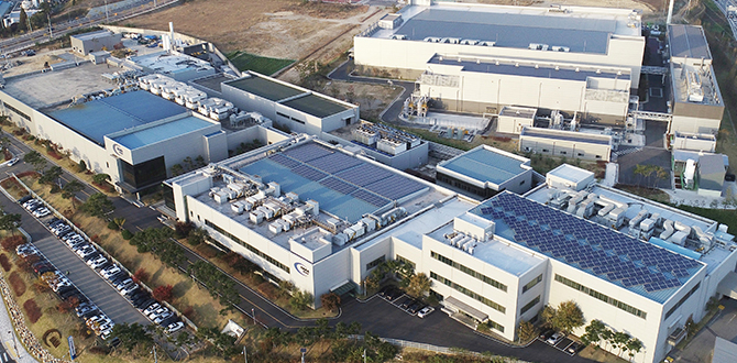
Hana Micron's chip packaging plant in Asan, South Korea. "We expect sales from our Vietnamese operations to come in at the trillion won range soon,” Lee said.
Memory chip packaging accounts for 70% of its sales revenue while packaging of system chips such as CPUs, application processors, fingerprint recognition sensors and automotive chips take up the rest.
“Eventually, we aim to raise the portion of system chips to 50% as they are less susceptible to market ups and downs,” said the CEO.
With a slowdown in the memory market over the past few years, Hana Micron’s 2023 operating profit is estimated at 66.3 billion won, down 36% from the previous year, according to financial research firm FnGuide.
“We expect our performance to improve this year, given growing demand for advanced chips from electronics makers and AI device makers,” Lee said.