Samsung’s new 2 nm foundry process to cut chip size by 17%

Intel is tipped to become the first chipmaker to apply the backside power delivery network to the 2-nanometer node

Samsung Foundry Forum (SFF) 2024 was held in San Jose, California in June
Jeong-Soo Hwang 1
2024-08-22 17:54:12 hjs@hankyung.com
Korean chipmakers

A new contract chipmaking technology, dubbed the backside power delivery network (BSPDN), will reduce the size of a 2-nanometer chip by 17%, compared with the traditional front-end power delivery technology, said Samsung Electronics Co.'s foundry business executive on Thursday.

The BSPDN, which Samsung is set to apply for mass production of the 2 nm process from 2027, also improves performance and power efficiency by 8% and 15%, respectively, compared to the chips with the front-end power delivery networks, said Lee Sungjae, vice president and Foundry PDK Development Team at Samsung.

He outlined the technological prowess of BSPDN in a keynote speech at Siemens EDA Forum 2024. It was the first time for a Samsung foundry business executive to give a detailed account of its BSPDN technology in public.

BSPDN is called a next-generation chip foundry technology. It places power rails on the back of the semiconductor wafer to eliminate bottlenecks between the power and signal lines, allowing for smaller chips.

Contract chipmakers are gearing up to adopt the advanced chipmaking process. Leading the pack, Intel plans to produce chips with BSPDN on the Intel 20A process, known as a 2 nm node, within the year. It dubbed its BSPDN technology as PowerVia.

TSMC, which controls 62% of the global foundry market, said it plans to introduce the BSPDN to its 1.6 nm and below process nodes around the end of 2026.

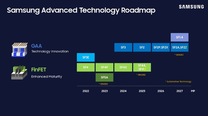
Samsung's advanced foundry process node roadmap unveiled at Samsung Foundry Forum (SFF) 2024

Lee also unveiled the roadmap and performance of chips to be made with the next-generation gate-all-around (GAA) technology that Samsung adopted in 2022 for the first time in the world.

It plans to mass-produce 3 nm chips based on the second-generation GAA technology (SF3) in the second half of this year and deliver GAA on its upcoming 2 nm process.

SF3 has improved chip performance and power efficiency by 30% and 50%, respectively, while reducing the chip size by 35%, compared with the chips produced on the first-generation GAA process, Lee added.

Write to Jeong-Soo Hwang at hjs@hankyung.com


Yeonhee Kim edited this article.

Samsung wins 2nm AI chip foundry, package order from Japan

Samsung wins 2nm AI chip foundry, package order from Japan

Choi Siyoung, Samsung Electronics' foundry chief, gives a keynote speech at Samsung Foundry Forum 2024 in Seoul on July 9 (Courtesy of Samsung Electronics) Samsung Electronics Co. announced on Tuesday it has bagged a 2-nanometer AI chip foundry and package turnkey order from Preferred Networks

Samsung unveils new foundry tech; AI chip sales to rise ninefold

Samsung unveils new foundry tech; AI chip sales to rise ninefold

Samsung’s foundry business chief Choi Si-young unveils new chipmaking tech at Samsung Foundry Forum (SFF) 2024 in San Jose SAN JOSE, Calif. – Samsung Electronics Co., the world’s largest memory chipmaker, on Wednesday unveiled a new contract chipmaking technology, with which i

Samsung, AMD to collaborate on 3 nm GAA tech chipmaking

Samsung, AMD to collaborate on 3 nm GAA tech chipmaking

AMD's headquarters in Santa Clara, California Samsung Electronics Co., the world’s largest memory chipmaker, is expected to expand its partnership with US-based fabless semiconductor designer Advanced Micro Devices Inc. (AMD) into cutting-edge 3-nanometer chip processing technology.For ye

Samsung on smooth track to 1.4 nm foundry tech to take on TSMC

Samsung on smooth track to 1.4 nm foundry tech to take on TSMC

Samsung’s foundry business chief Choi Si-young unveils a new chipmaking roadmap at Samsung Foundry Forum (SFF) 2023 SILICON VALLEY  – Samsung Electronics Co., the world’s largest memory chipmaker, on Tuesday unveiled details of its advanced process roadmap to take on its

Samsung to make 2-nanometer GAA chips by 2025 to overtake TSMC

Samsung to make 2-nanometer GAA chips by 2025 to overtake TSMC

Samsung Foundry Forum 2021 logo Samsung Electronics Co. said on Thursday it will be able to commercialize a 2-nanometer transistor process technology by 2025 to take on bigger foundry rival Taiwan Semiconductor Manufacturing Co. (TSMC) at the leading edge of chip processing.At the Samsung Found

(* comment hide *}