Samsung Electronics Co. plans to more than double its total semiconductor investment in Texas to about $44 billion to add an advanced semiconductor factory and a packaging facility near its foundry plant under construction, the Wall Street Journal reported on Friday.
The spending plan is more than double the $17 billion it pledged in 2021 to build a foundry plant in Taylor, Texas, near its existing operations in Austin, by the end of this year. At the time, that marked Samsung’s largest-ever investment in the US.
The additions of a semiconductor factory and a packaging plant are estimated to cost $20 billion and $4 billion, respectively, according to the report.
The world’s largest memory chipmaker is scheduled to announce the new investment plan on April 15, the newspaper reported, citing unnamed sources.
Once the $44 billion investment is completed, its semiconductor complex in Texas will be fully equipped to provide one-stop service from foundry to packaging to US-based fabless companies, or chip designers such as Nvidia Corp. and AMD Inc.
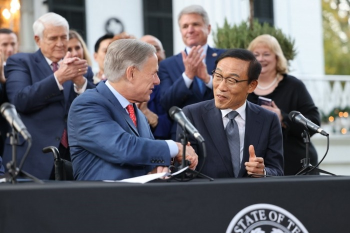
In November 2021, Texas Governor Greg Abbott (left) and Kim Ki-nam, then-vice chairman of Samsung Electronics, announce a $17 billion plant deal “One-stop service is the greatest strength that Samsung Electronics can provide to its customers as a comprehensive semiconductor company,” said a semiconductor industry official.
The increased spending will also be used to build an R&D facility at the Samsung semiconductor hub in Texas, which is expected to collaborate with the University of Texas at Austin, a top engineering school in the US.
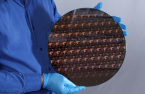
The semiconductor market is mainly divided into foundry and packaging services.
Foundry companies assemble customized semiconductor chips for chip designers. Samsung trails Taiwan's TSMC Co., which controls over half of the foundry market.
Packaging is one of the final steps in semiconductor manufacturing. In the process, graphic processing units (GPU) are combined with high-performance DRAMs such as high bandwidth memory (HBM) to operate as a single chip.
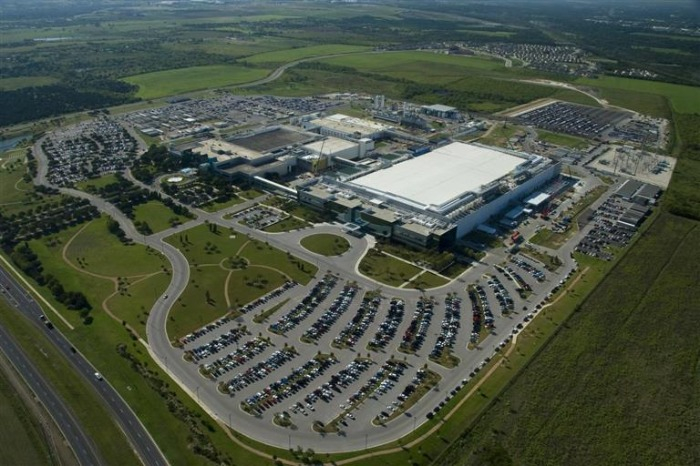
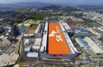
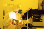
A Samsung Electronics semiconductor plant in Austin, Texas US SUBSIDIES
If Samsung ramps up its investment in Texas to $44 billion, it is expected to qualify for over $6 billion in subsidies from the US government under the US Semiconductor Support Act, according to the Wall Street Journal report.
Last month, Bloomberg News reported that Samsung is expected to receive more than $6 billion in US chip subsidies -- more than expected -- on the condition that it commits to extra US investments beyond the ongoing project in Texas.
Its aggressive investment is expected to gain momentum from stronger-than-expected first-quarter results, with the semiconductor market showing signs of recovery after a one-and-half-a-year slump.