Samsung to launch 3D HBM chip packaging service in 2024

The chipmaker is expected to package HBM4 chips to be rolled out next year on a turnkey basis

Samsung Foundry Forum 2024 held in San Jose, California on June 12-13
Jeong-Soo Hwang 2
2024-06-16 13:43:23 hjs@hankyung.com
Korean chipmakers

SAN JOSE -- Samsung Electronics Co. will launch three-dimensional (3D) packaging services for high-bandwidth memory (HBM) within the year, a technology expected to be introduced for the artificial intelligence chip’s sixth-generation model HBM4 due in 2025, according to the company and industry sources.

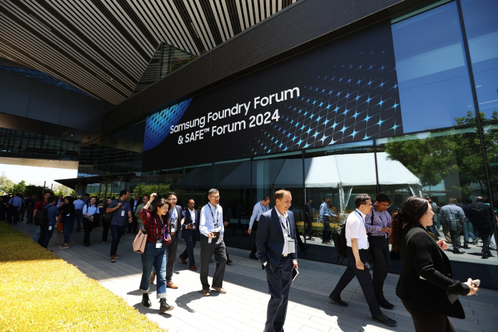
On June 20, the world’s largest memory chipmaker unveiled its latest chip packaging technology and service roadmap at the Samsung Foundry Forum 2024 held in San Jose, California.

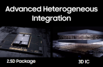
It was the first time Samsung released the 3D packaging technology for HBM chips at a public event. Currently, HBM chips are packaged mainly with 2.5D technology. 

The release came about two weeks after Nvidia co-founder and Chief Executive Jensen Huang unveiled the new-generation architecture of its AI platform Rubin during a speech in Taiwan.

HBM4 will likely be embedded in Nvidia’s new Rubin GPU model expected to hit the market in 2026.

VERTICAL CONNECTION

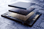
Samsung’s latest packaging technology features HBM chips stacked vertically on top of a GPU to further accelerate data learning and inference processing, a technology regarded as a game changer in the fast-growing AI chip market.

Currently, HBM chips are horizontally connected with a GPU on a silicon interposer under 2.5D packaging technology.

By comparison, 3D packaging does not require a silicon interposer, a thin substrate that sits between chips to facilitate their communication and working together.

Samsung dubs its new packaging technology as SAINT-D, short for Samsung Advanced Interconnection Technology-D.

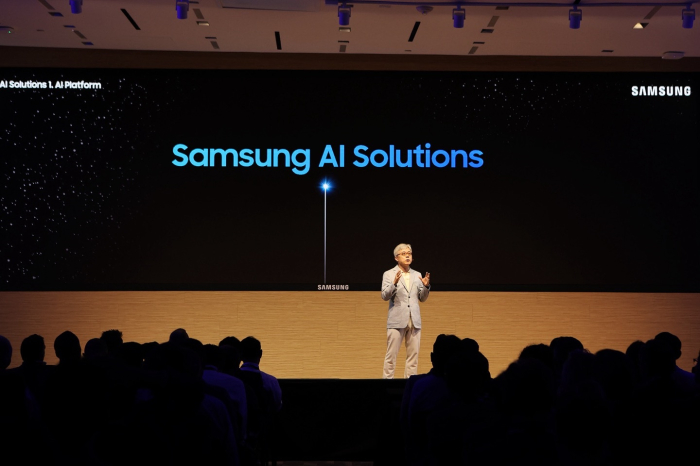
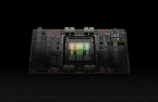
Samsung’s foundry business chief Choi Si-young unveils new chipmaking technology at Samsung Foundry Forum (SFF) 2024 in San Jose

TURNKEY SERVICE

The South Korean company is understood to offer 3D HBM packaging on a turnkey basis.

To do so, its advanced packaging team will vertically interconnect HBM chips produced at its memory business division with GPUs assembled for fabless companies by its foundry unit.

“3D packaging reduces power consumption and processing delays, improving the quality of electrical signals of semiconductor chips,” said a Samsung Electronics official.

In 2027, Samsung plans to introduce all-in-one heterogeneous integration technology that incorporates optical elements that dramatically increase the data transmission speed of semiconductors into one unified package of AI accelerators.

In line with the growing demand for low-power, high-performance chips, HBM is projected to make up 30% of the DRAM market in 2025 from 21% in 2024, according to TrendForce, a Taiwanese research company.

MGI Research forecast the advanced packaging market, including 3D packaging, to grow to $80 billion by 2032, compared with $34.5 billion in 2023.

Write to Jeong-Soo Hwang at hjs@hankyung.com

Yeonhee Kim edited this article. 

Samsung unveils new foundry tech; AI chip sales to rise ninefold

Samsung unveils new foundry tech; AI chip sales to rise ninefold

Samsung’s foundry business chief Choi Si-young unveils new chipmaking tech at Samsung Foundry Forum (SFF) 2024 in San Jose SAN JOSE, Calif. – Samsung Electronics Co., the world’s largest memory chipmaker, on Wednesday unveiled a new contract chipmaking technology, with which i

SK Hynix to build advanced packaging plant in Indiana for $3.9 bn

SK Hynix to build advanced packaging plant in Indiana for $3.9 bn

SK Hynix Inc., the world’s leading high bandwidth memory (HBM) chip producer, will plow in $3.87 billion to build advanced packaging and research and development facilities for AI chips in Indiana, which would be the first of its kind in the US and the company’s first overseas HBM

Samsung to build $281 million chip packaging R&D center in Yokohama

Samsung to build $281 million chip packaging R&D center in Yokohama

A researcher at a Samsung Electronics chip cleanroom South Korea’s Samsung Electronics Co., the world’s largest memory chipmaker, will build a 40 billion yen ($281 million) advanced chip packaging research and development center in Japan amid improving ties between the neighboring c

Samsung to relocate packaging unit workplace to lure talent

Samsung to relocate packaging unit workplace to lure talent

(Courtesy of Samsung Electronics) Samsung Electronics Co., the world’s top memory chipmaker, is set to relocate its advanced packaging department’s workplace in South Korea to retain employees at and attract talent to the priorized unit amid the boom in artificial intelligence.Samsu

Samsung to unveil 3D AI chip packaging tech SAINT to rival TSMC

Samsung to unveil 3D AI chip packaging tech SAINT to rival TSMC

Samsung rapidly advances its 3D chip packaging tech Samsung Electronics Co., the world’s largest memory chipmaker, plans to unveil an advanced three-dimensional (3D) chip packaging technology next year to compete with foundry leader Taiwan Semiconductor Manufacturing Company (TSMC).The Su

Samsung set to supply HBM3, packaging services to AMD

Samsung set to supply HBM3, packaging services to AMD

Image of Samsung Electronics' HBM3 chip (Courtesy of Samsung) South Korea’s Samsung Electronics Co., the world’s top memory chipmaker is poised to provide its high bandwidth memory (HBM) chips and turnkey packaging services to US-based fabless semiconductor designer Advanced Micro D

Samsung Elec to provide HBM3, packaging service to Nvidia

Samsung Elec to provide HBM3, packaging service to Nvidia

H100 Tensor Core GPU (Courtesy of Nvidia) Samsung Electronics Co., the world’s top memory chipmaker, is set to provide high-performance semiconductors and packaging service to the global chip designer Nvidia Corp. for its graphics processing units, adding to expectations that the South Ko

SK to build first chip packaging plant in US with $22 bn investment

SK to build first chip packaging plant in US with $22 bn investment

US President Joe Biden waves at visiting SK Group Chairman Chey Tae-won at the White House. The two met through a video conference call as Biden continues to recover from COVID-19. WASHINGTON DC – SK Group, South Korea’s second-largest conglomerate, said on Wednesday it will build i

(* comment hide *}