Samsung to launch low-power, high-speed AI chips in 2024

It will also unveil advanced three-dimensional (3D) chip packaging next year

(Courtesy of Getty Images)
Jeong-Soo Hwang and Ik-Hwan Kim 2
2023-11-21 21:57:43 hjs@hankyung.com
Korean chipmakers

Samsung Electronics Co. will launch low latency wide (LLW) DRAMs next year, designed to improve the power efficiency of artificial intelligence applications by 70% more than that of regular DRAMs, the company said at its annual investors forum last week.

LLW DRAMs will become its flagship, next-generation chips and be embedded into AI devices such as extended reality headsets. Samsung aims to beef up artificial intelligence chip foundry sales to about 50% of its total foundry sales in five years.

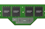
The new AI chips will enhance data processing speed and capacity by increasing the number of input/output terminals (I/O) in a semiconductor circuit, compared with existing DRAMs.

(Courtesy of Getty Images)

3D PACKAGING

Next year, the world’s No. 1 memory chipmaker will unveil an advanced three-dimensional (3D) chip packaging technology, including the most advanced 3.5D packaging, the company said during the IR event.

It increases the processing speed and data processing capacity of electronic devices by stacking processors such as the central processing unit (CPU) and graphics processing unit (GPU) vertically with high-bandwidth memory (HBM) chips.

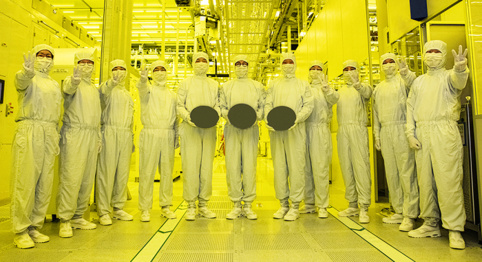
Samsung employees hold semiconductor wafers made with 3-nanometer technology

3 NM PROCESS

Samsung also will further sharpen its 3-nanometer chip processing technology, currently the industry’s smallest and most advanced process node, to be suitable for AI applications.

Last year, it began the mass production of 3 nm chips for fabless clients as a global first and ahead of Taiwan’s TSMC Co.

Earlier this year, Samsung was said to have significantly advanced the production yields of its first-generation 3 nm process technology to “a perfect level.”

“We can increase (memory chips’) performance by 2.2 times every two years,” said Jeong Ki-bong, vice president of Samsung Foundry, the foundry semiconductor business of Samsung Electronics, told investors at the IR event.

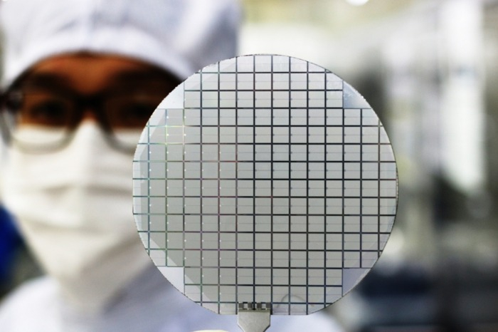
A semiconductor wafer

GDP STRATEGY

At the investors forum, Samsung presented the initials of GAA, dram and packaging, or GDP, as the keyword for its new strategy.

GAA, short for gate-all-around, reduces the leakage current of processors with a circuit width of 3 nm or below. It is Samsung’s key architecture to develop next-generation DRAMs and packaging technology.

The 3 nm technology is the first process node on which Samsung applied its first-generation GAA structure transistors.

IN COLLABORATION WITH TESLA

Samsung is working with Tesla Inc. to develop the EV maker’s next-generation Full Self-Driving (FSD) chips for Level-5 autonomous driving vehicles.

Waymo's robot taxi in pilot operation in Phoenix, Arizona

Samsung recently hired YoonJung Ahn, a design head at Waymo, Alphabet’s autonomous driving technology unit, as executive vice president to lead the design management center.

The chipmaker also plans to develop a 4 nm AI accelerator, a high-performance computing machine used to process AI workloads.

According to market research firm Omdia, the AI ​​semiconductor market, estimated at $55.3 billion this year, is expected to reach $112 billion by 2027.

Write to Jeong-Soo Hwang and Ik-Hwan Kim at hjs@hankyung.com
 

Yeonhee Kim edited this article.

Samsung Electronics to up AI chip foundry sales to 50% by 2028

Samsung Electronics to up AI chip foundry sales to 50% by 2028

Employees at Samsung Foundry Business and Semiconductor R&D Center pose for a photo, celebrating Samsung's first-ever production of the 3 nm process with GAA architecture (Courtesy of Samsung Electronics) Samsung Electronics Co. plans to up artificial intelligence chip foundry sales to abou

Samsung to unveil 3D AI chip packaging tech SAINT to rival TSMC

Samsung to unveil 3D AI chip packaging tech SAINT to rival TSMC

Samsung rapidly advances its 3D chip packaging tech Samsung Electronics Co., the world’s largest memory chipmaker, plans to unveil an advanced three-dimensional (3D) chip packaging technology next year to compete with foundry leader Taiwan Semiconductor Manufacturing Company (TSMC).The Su

On-device AI chips: New battleground for chipmakers

On-device AI chips: New battleground for chipmakers

As on-device artificial intelligence, designed for smart gadgets such as smartphones, laptops and autonomous-driving cars, emerges as a mega-trend for the AI industry, global chipmakers are upping the ante in the race to produce AI-enabled memory chips.Compared with generative AI such as ChatG

Samsung showcases HBM3E DRAM, automotive chips

Samsung showcases HBM3E DRAM, automotive chips

SILICON VALLEY -- Samsung Electronics Co. on Friday showcased a number of new-concept, next-generation DRAM chips, including the industry’s most advanced HBM3E, alleviating market concerns that it might trail local rival SK Hynix Inc. in the super-giant AI chip market.At Samsung Memory T

Samsung Elec to launch HBM4 in 2025 to win war in AI sector

Samsung Elec to launch HBM4 in 2025 to win war in AI sector

Hwang Sang-joon, executive vice president of DRAM product & technology at Samsung (Courtesy of Samsung) Samsung Electronics Co., the world’s top memory chipmaker, aims to introduce sixth-generation top-performance High Bandwidth Memory4 (HBM4) DRAM chips in 2025 to win the intensifyin

Samsung set to keep supremacy in low power DRAM with game changer

Samsung set to keep supremacy in low power DRAM with game changer

Samsung Electronics' LPCAMM (Courtesy of Samsung Electronics)  South Korea’s No. 1 memory chip maker Samsung Electronics Co., also the world’s top player, is set to further break away from the pack with advanced memory chip products that are expected to bring a paradigm shift t

Samsung set to supply HBM3, packaging services to AMD

Samsung set to supply HBM3, packaging services to AMD

Image of Samsung Electronics' HBM3 chip (Courtesy of Samsung) South Korea’s Samsung Electronics Co., the world’s top memory chipmaker is poised to provide its high bandwidth memory (HBM) chips and turnkey packaging services to US-based fabless semiconductor designer Advanced Micro D

Samsung Elec to provide HBM3, packaging service to Nvidia

Samsung Elec to provide HBM3, packaging service to Nvidia

H100 Tensor Core GPU (Courtesy of Nvidia) Samsung Electronics Co., the world’s top memory chipmaker, is set to provide high-performance semiconductors and packaging service to the global chip designer Nvidia Corp. for its graphics processing units, adding to expectations that the South Ko

Samsung to make 3 nm chips for Nvidia, Qualcomm, IBM, Baidu

Samsung to make 3 nm chips for Nvidia, Qualcomm, IBM, Baidu

Samsung executives hold semiconductor wafers made with 3-nanometer tech Samsung Electronics Co., the world’s largest memory chipmaker, will make semiconductors with the industry’s most advanced 3-nanometer process node for its clients, including Nvidia, Qualcomm Technologies, IBM an

Samsung's 3 nm chip narrows microchip gap with TSMC

Samsung's 3 nm chip narrows microchip gap with TSMC

Samsung Electronics' employees show the industry's smallest chip using the 3 nm process node Samsung Electronics Co. has kicked off mass production of 3-nanometer chips based on the industry’s smallest process node as a global first, a move expected to narrow its gap with TSMC Co. in the

(* comment hide *}