Korea to inject $200 mn into semiconductor packaging R&D

South Korea lags far behind Taiwan, China and US in the semiconductor packaging market

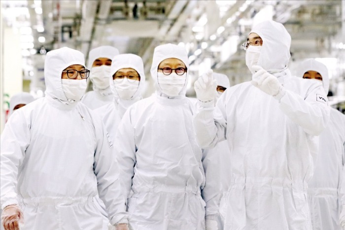
Samsung Electronics Chairman Jay Y. Lee (far right) inspects the semiconductor packaging line at the Samsung Cheonan Factory in Cheonan, Korea (Courtesy of Samsung) 
Yeong-Hyo Jeong 2
2024-06-26 17:28:21 hugh@hankyung.com
Korean chipmakers

South Korea will inject 274.4 billion won ($200 million) into a state-run R&D project for semiconductor packaging technology, a key to producing the high-performance, low-power chips essential for AI applications.

The government spending aims to narrow the gap with Taiwan, China and the US in the semiconductor back-end process market, where Korea controls less than 10%. In contrast, it commands 60% of the memory chip market as of 2022, according to the Ministry of Science and ICT.

The Ministry of Trade, Industry and Energy said on Wednesday the R&D spending plan had passed the preliminary feasibility test conducted by the science ministry. That means the government has given the go-ahead to the seven-year project running until 2031.

The plan represents a follow-up to a 65-billion-won, state-run project on semiconductor packaging R&D undertaken between 2018 and 2022.

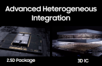
Packaging refers to assembling different types of semiconductor chips and providing them to customers in one piece.

The process involves detaching chips through wafer sawing and mounting the chips on a module that will be installed onto a motherboard. The package allows the chips to be electrically and mechanically connected to external components.

To meet the growing demand for high-end chips such as high bandwidth memory (HBM) amid the AI boom, chipmakers are focusing on improving back-end processing or packaging technology now that semiconductor miniaturization has reached its physical limits.

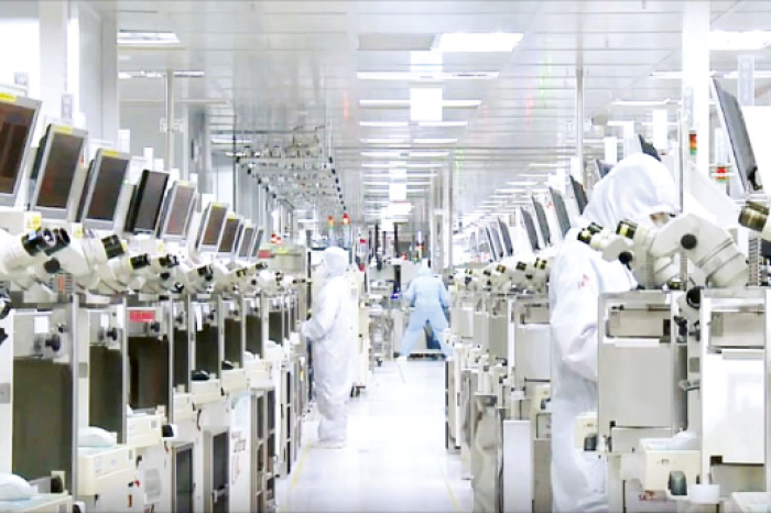
An SK Hynix semiconductor packaging line (Courtesy of SK Hynix)

The advanced semiconductor packaging market is forecast to expand at a compounded annual growth rate of 10% to $78.6 billion by 2028, from $44.3 billion in 2022, according to research company Yole.

Samsung Electronics will launch three-dimensional (3D) packaging services for HBM chips within the year, according to the company and industry sources earlier this month.

To do so, its advanced packaging team will vertically interconnect HBM chips produced at its memory business division with GPUs assembled for fabless companies by its foundry unit.

3D packaging reduces power consumption and processing delays, improving the electrical signal quality of semiconductor chips.

Presently, HBM chips are horizontally connected with a GPU on a silicon interposer via the 2.5D packaging process.

Write to Yeong-Hyo Jeong at hugh@hankyung.com
Yeonhee Kim edited this article

Booming AI industry boosts chip packaging equipment makers

Booming AI industry boosts chip packaging equipment makers

Hanmi Semiconductor CEO & Vice Chairman Kwak Dong Shin showcases its product on April 7, 2022, at its headquarters in South Korea (File photo by Moon-Chan Hur) Global chip packaging equipment manufacturers are enjoying surging demand and skyrocketing share prices thanks to the rapid growth

Samsung to launch 3D HBM chip packaging service in 2024

Samsung to launch 3D HBM chip packaging service in 2024

Samsung Foundry Forum 2024 held in San Jose, California on June 12-13 SAN JOSE -- Samsung Electronics Co. will launch three-dimensional (3D) packaging services for high-bandwidth memory (HBM) within the year, a technology expected to be introduced for the artificial intelligence chip&rsquo

SK Hynix to build advanced packaging plant in Indiana for $3.9 bn

SK Hynix to build advanced packaging plant in Indiana for $3.9 bn

SK Hynix Inc., the world’s leading high bandwidth memory (HBM) chip producer, will plow in $3.87 billion to build advanced packaging and research and development facilities for AI chips in Indiana, which would be the first of its kind in the US and the company’s first overseas HBM

Hana Micron to develop 2.5D packaging for Nvidia’s H100 AI chip: CEO

Hana Micron to develop 2.5D packaging for Nvidia’s H100 AI chip: CEO

Hana Micron CEO Lee Dong-cheol With burgeoning demand for high-performance artificial intelligence chips, back-end process technology, which assembles various semiconductors and tests the functionality of such chips, has become more important than ever.So, it’s no wonder leading contract

Samsung to build $281 million chip packaging R&D center in Yokohama

Samsung to build $281 million chip packaging R&D center in Yokohama

A researcher at a Samsung Electronics chip cleanroom South Korea’s Samsung Electronics Co., the world’s largest memory chipmaker, will build a 40 billion yen ($281 million) advanced chip packaging research and development center in Japan amid improving ties between the neighboring c

Samsung to relocate packaging unit workplace to lure talent

Samsung to relocate packaging unit workplace to lure talent

(Courtesy of Samsung Electronics) Samsung Electronics Co., the world’s top memory chipmaker, is set to relocate its advanced packaging department’s workplace in South Korea to retain employees at and attract talent to the priorized unit amid the boom in artificial intelligence.Samsu

Samsung to unveil 3D AI chip packaging tech SAINT to rival TSMC

Samsung to unveil 3D AI chip packaging tech SAINT to rival TSMC

Samsung rapidly advances its 3D chip packaging tech Samsung Electronics Co., the world’s largest memory chipmaker, plans to unveil an advanced three-dimensional (3D) chip packaging technology next year to compete with foundry leader Taiwan Semiconductor Manufacturing Company (TSMC).The Su

Samsung set to supply HBM3, packaging services to AMD

Samsung set to supply HBM3, packaging services to AMD

Image of Samsung Electronics' HBM3 chip (Courtesy of Samsung) South Korea’s Samsung Electronics Co., the world’s top memory chipmaker is poised to provide its high bandwidth memory (HBM) chips and turnkey packaging services to US-based fabless semiconductor designer Advanced Micro D

Samsung Elec to provide HBM3, packaging service to Nvidia

Samsung Elec to provide HBM3, packaging service to Nvidia

H100 Tensor Core GPU (Courtesy of Nvidia) Samsung Electronics Co., the world’s top memory chipmaker, is set to provide high-performance semiconductors and packaging service to the global chip designer Nvidia Corp. for its graphics processing units, adding to expectations that the South Ko

(* comment hide *}