Global chip packaging equipment manufacturers are enjoying surging demand and skyrocketing share prices thanks to the rapid growth of the artificial intelligence industry.
South Korean Hanmi Semiconductor Co., Japanese Disco Corp. and Dutch BE Semiconductor Industries N.V. (Besi) are key beneficiaries as
chip packaging – putting chips into protective casing and connecting them with power and other components – has become more important amid difficulties in the development of ultra-fine process technology of one nanometer or less despite the fast expansion of AI, which requires faster chips.
The H100, the global AI chip leader Nvidia Corp.’s graphics processing unit (GPU) chip, maximizes its performance through packaging processes.
“Some customers asked us to establish production lines and manufacture sufficient equipment, saying they would make payments in advance,” said a chip equipment maker official.
Such a boom has bolstered their share prices. Hanmi’s stock price has nearly tripled so far this year to 175,400 won ($126.3) as of Monday, while Disco’s shares have almost doubled to 63,200 yen ($395.7).
The global chip packaging equipment industry has been expected to grow rapidly, industry sources said. The sector was forecast to increase 48.8% to $61 billion by 2028 from $41 billion last year, according to the semiconductor information platform Techinsights Inc. That compared with 35.8% growth in chip equipment for the entire processes.
DOMINATES WAFER GRINDER, DICING SAW MARKETDisco CEO Kazuma Sekiya has made more business trips this year than usual, mostly to seek clients’ understanding as the Japanese company has yet to supply as many products as customers wanted.
Disco, founded in 1937, manufacturers wafer grinders and wafer dicing saws, accounting for about 70% of the global market.
Its operating income for the fiscal year ended on March 31 rose 10% to 121.5 billion yen as sales grew 8.2% to 307.6 billion yen.
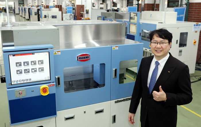
TO SIGN DEALS WITH SAMSUNG AFTER MICRONHanmi is strong in making thermal compression (TC) bonders, an essential device for high bandwidth memory (HBM) chips that attach semiconductor chips to substrates through thermal compression.
The South Korean company is increasing its customer base.
The supplier to SK Hynix Inc., the world’s second-largest memory chipmaker, agreed to ink a 22.6 billion won TC bonder deal with Micron Technology Inc. in April.
Hami is expected to sign similar contracts with Samsung Electronics Co., the world’s top memory chipmaker.
HYBRID BONDINGBesi is the world’s top manufacturer of die attach systems used in the semiconductor industry to attach a silicon chip to the die pad of a semiconductor package's support structure, such as a leadframe or metal can header. The company has a market share of 40%.
Besi, the so-called hope of the Dutch semiconductor equipment industry to succeed the world’s biggest maker of semiconductor equipment, ASML Holdings N.V., secured a rock-solid position in the hybrid-bonding system, which will be applied to the HBM4 to be manufactured next year.
Hybrid bonding is a new assembly technique that aids in the connection of multiple chipsets using direct copper interconnects. It allows for an increase in chip contact density. As the lengths of interconnected wiring are shorter, it is much easier to build 3D structures.
Besi announced in May that it won an order for hybrid bonding systems from a leading semiconductor logic manufacturer. The order is for the company’s latest generation system incorporating 100-nanometer (nm) placement accuracy.
Write to Jeong-Soo Hwang at
hjs@hankyung.com
Jongwoo Cheon edited this article.